Reverse engineering Google's TPUs
TL;DR: we built a simulator of Google's TPUs that runs the real, unmodified TPU software stack, and a website where you can send us a JAX program and get back a cycle-level trace of what the chip would do with it. Along the way we learned a lot about how TPUs work that is not public.
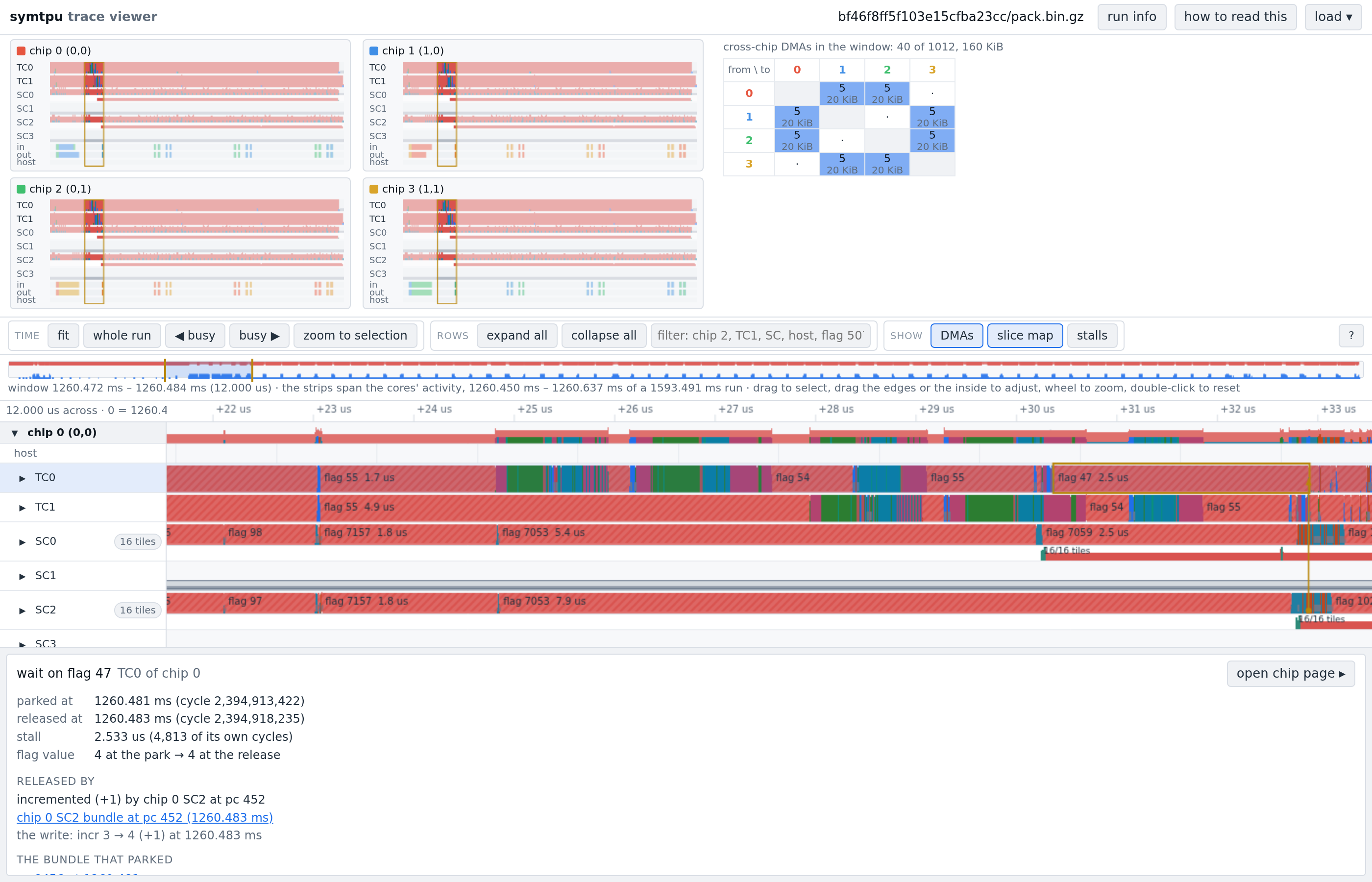
At Gherkin Labs we aim to make machine learning more efficient. We started at the bottom of the stack, with Google's TPUs. Unlike Nvidia GPUs there is very little public technical information about them. TPUs are tied to Google's stack. For a long time JAX was the only option to use them. Most recently work has been done to improve support in Torch, but both end up going through the same compiler. That lack of information makes it hard to extract every ounce of performance from the hardware, and it makes it hard for anyone but Google to build tooling for it.
We reverse engineered the full communication protocol between the TPU driver and the TPU hardware: how data is transferred to and from the chip, how programs are packed for the tensor cores and the sparse cores, and how chips are configured to talk to each other within a pod and between pods. "Full" applies to the protocol, not to the chip: we do not claim to know every inner detail of a TPU, such as the exact timing of a DMA or the bit-exact behaviour of every arithmetic unit.
What we have built
We could have built a TPU driver first, but instead we built a simulator. It presents
itself as a shared library, libsymtpu.so. Loaded with LD_PRELOAD, any program
sees a number of virtual TPU devices that expose the same interfaces and protocols as
real ones. They decode the instruction streams and simulate both tensor cores and
sparse cores on the CPU. A virtual TPU is cheap: a few megabytes of RAM, more if the
program needs a lot of HBM, so large topologies can be simulated on one machine.
The traces are cycle-level because the TPU itself is. The chip issues exactly one instruction bundle per cycle and almost every instruction has a fixed, documented latency, so the compiler decides the cycle each instruction runs on before the program ever reaches the hardware. Replaying the compiler's schedule is therefore replaying the chip's timing. The parts the simulator has to model rather than replay are the three things whose duration is not fixed by the schedule: the time a DMA takes between two memories, the time a message takes between two chips, and the cost of reading and writing sync flags.
Why this matters
There is a lot of pressure to make machine learning more efficient, GPU clusters are getting harder to obtain, and the alternative accelerators are bottlenecked on documentation and availability. TPUs are comparatively easy to get but aren't really documented. Our goal is to understand TPUs well enough to unlock them fully.
We also believe low-level kernel engineering is changing shape. Traditional compiler pipelines get "good enough" performance. LLM-driven kernel search can go further, but only with a strong harness and a way to evaluate and trace every generated kernel. A fast, faithful simulator with cycle-level traces is that harness.
The rest of this post is the tour of the machine. Sizes and bundle layouts are collected in the appendix at the end.
What we have learned
We will focus on TPU v7 (v7x, codename Ironwood). Google's own diagram is a good starting point:
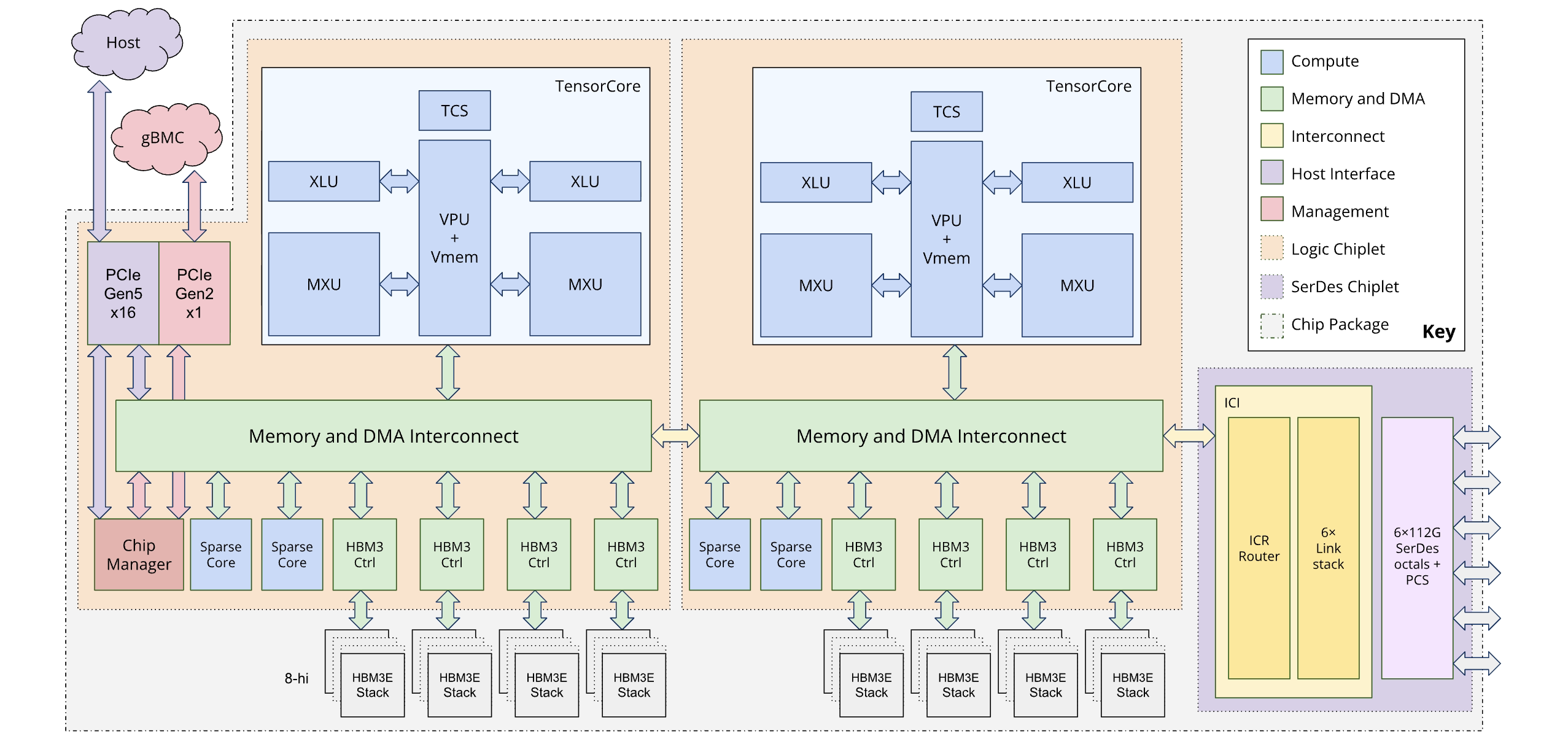
A v7 chip is two dies, each with one tensor core and two sparse cores, and the two halves share the chip's HBM. A tensor core is made of an MXU (matrix multiply unit), an XLU (cross lane unit), a VPU (vector processing unit) and a scalar unit that drives them. DMA engines move data between the levels of the memory hierarchy, HBM included. Chips talk to their neighbours over ICI links, and packets are routed hop by hop through routing tables.
In technical terms, TPUs are VLIW machines. Chip design, like everything, is about compromise. On one side you can build processors that are clever and make the compiler's life easy, like Intel's: the instruction set is large and convoluted, but the hardware tracks instruction dependencies itself. On the other side you can make the processor dumb and move the complexity into the compiler. TPUs are the latter. Every cycle each core executes one bundle. A bundle is a fixed set of slots. Each slot holds one instruction for one execution unit, all issued in parallel. It is the compiler's job to fill the slots and to schedule them correctly and at the right time. That compiler ships inside Google's TPU driver. JAX, Torch and Pallas all go through it, and at the time of writing it is next to impossible to assemble TPU programs by hand.
Compared to a GPU the memory hierarchy is lightweight and entirely explicit. There are no caches, no coherence and no hardware-managed levels: every memory is a scratchpad with a fixed address, and "shared" always means an explicit transfer plus a flag. Each core has its own vector memory, scalar memory, instruction memory and bank of sync flags, and nothing reads HBM directly: data reaches a core only by DMA or, on the sparse core, by stream. The exact sizes are in the appendix.
Tensor core
Purpose
The tensor core exists to keep its matrix units fed, because that is where the flops are. Everything else in it is there to get data into the right shape for the arrays and to glue matrix multiplications together. This includes elementwise arithmetic on vectors, moving vectors between memory and registers, and control flow.
The unit of computation is a vector. A vector register holds 8 sublanes of 128 32-bit values, so 1024 f32 per register, and every vector instruction works on a whole register at once. There are 64 of them, backed by 64 MiB of vector memory (VMEM) that loads and stores address directly and that DMAs fill from HBM.
The MXU is a systolic array: a 256 x 256 grid of multiply-accumulate cells. The weights are loaded into the grid once, then activations flow through it one row per cycle, each cell multiplying what passes by with the weight it holds and passing the partial sum to its neighbour. No value is fetched from memory more than once, which is what makes the array so efficient. Google's write-up of the first TPU has a good illustration.
There are two MXUs per tensor core. The XLU manipulates whole registers: transpose, rotate, permute and cross-lane reductions.
Sync flags are best understood as a mix of atomics and condition variables. An asynchronous operation (a DMA, a message from another core) adds to a flag when it completes, and the core has an instruction to sleep until a flag reaches a value. The core cannot load from HBM; every access to it is a DMA into VMEM or the scalar memory, and the DMA reports completion through a sync flag.
How work flows
A matrix multiply is three steps. The core pushes the weight tile into the array, which latches it. It then streams 8 x 128 slices of the activations through the array, one push per bundle. The products accumulate in a matrix result buffer, and the core pops finished rows out of it into registers a fixed number of cycles later. The transcendental unit and the XLU work the same way: push now, pop later. This is why the bundle has dedicated result slots.
Most instructions have a fixed latency and the compiler schedules every bundle statically: a load's result is used exactly N bundles later, and a pop is placed where the result is due.
Programs are limited to 65536 bundles, and there is no instruction cache. When a program is bigger than that the compiler splits it into overlays: the code DMAs the next section from HBM into instruction memory and jumps to it.
Sparse core
Purpose
The sparse core has a very different job. A tensor core is built to keep a 256 x 256 multiplier array fed with dense tiles. It is very good at that and bad at anything made of data-dependent decisions. Embedding lookups, recommendation models and deduplication are exactly that, and they are at the heart of many production workloads. That is where the sparse core fits.
A sparse core is 17 small cores: one sequencer and 16 tiles.
- The sequencer is a scalar processor: 32 registers, integer and float arithmetic, branches, a DMA engine, sync flags, and no vector unit at all. Its job is orchestration. It receives work from the host or the tensor core, moves blocks of data around with DMAs, launches tasks on the tiles, and waits for them to finish.
- A tile is a complete small machine: the same scalar processor as the sequencer, plus a narrow vector unit (64 registers of 16 x 32-bit values, no sublanes), a stream engine, a cross-lane unit, and private memory. Sixteen tiles run sixteen independent instruction streams, which is how the core keeps enough memory requests in flight to hide HBM latency.
How work flows: tasks
The sequencer writes a task's arguments (table address, id list address, output
address, counts) into a small argument file called the dregs, then issues a
task_request. Every tile receives its own copy of the arguments and starts the same
code. The split of the work is decided by the compiler as a function of the tile id:
each tile reads its id and derives its own range of the data from it and from the
arguments, so no tile has to be told what to do at run time. When a tile is done it
adds one to a sync flag in the sequencer's flag bank; the sequencer sleeps on that
flag until all sixteen have reported, then launches the next task or signals the
tensor core. Tiles never launch other tiles; they only exchange data and flags among
themselves.
Tile code lives in a 16384-bundle instruction memory shared by the 16 tiles, with a small per-tile prefetch buffer in front of it. Each task is DMA'd from HBM into it before it runs, and a running task typically prefetches the next one while it works.
How a tile moves data: streams
The only way for a tile to load data into its own tile memory (TileSpmem, 8192
vectors) is through a stream instruction. A stream is a DMA with vector shaped
semantics, in either direction between tile memory and HBM. It can move a linear or
strided block, or it can be indirect: given a vector of row indices [a, b, c, d] in a
register, one stream gathers rows a, b, c and d from a table in HBM into the tile's
memory. In the other direction the indirect form can scatter-add: each row streamed
out is added into the destination row its index names.
Streams are asynchronous. The tile issues one, moves on, and later waits on a sync flag for the number of words it asked for. A tile usually has several in flight.
How a tile computes: the vector unit and the cross-lane unit
Once rows are in tile memory, the vector ALU does the arithmetic on 16-wide registers: sums of rows, scaling, converts, compares into masks, selects. The distinctive piece is the cross-lane unit. Where the tensor core's XLU rotates and transposes, the tile's does scans, sorts and uniquify over the 16 lanes of a register:
- inclusive scans: prefix add, min and max, with the total in the last lane, plus index-returning forms that yield an argmax or argmin;
- segmented scans: the same, restarting at every lane the mask marks as a segment boundary;
- sort: 16 keys ascending or descending, with the permutation;
- uniquify: for each lane, how many times its value has been seen so far, and a mask of last occurrences.
Like the tensor core's MXU, these instructions do not write their result to a register. They push it into one of three small result queues, and a later bundle pops it. In the compiled programs the pop shares its bundle with other work, so it costs no issue cycle, and a burst of pushes can wait in the queue until there is a register to receive them.
How a tile pipelines: circular buffers
Every tile has 16 circular buffer registers, or cbregs. Each holds a base address, a size and a cursor, and any load, store or stream can name one: the address is then the cursor plus the instruction's own offset, wrapped into the ring by hardware, and an "update" form advances the cursor by the number of words moved.
They solve a problem specific to this kind of workload: the amount of data per partition is only known at run time, and the tile's memory is a fixed scratchpad. Used correctly these rings can be used to interleave different work streams and amortize memory accesses.
How we know
We've based our work on top of static reverse engineering of Google's TPU driver. First by doing manual reverse engineering to understand the different communication protocols and then by writing this simulator. The simulator allowed us to run the real stack without interacting with TPUs directly. LLMs were a great help to design JAX programs that we could then run through our simulator and compare its results with the one of a CPU reference.
The timing side needs no separate validation for the bulk of the instruction set: the driver ships the per-instruction latency tables its own scheduler uses, and the simulator replays the schedule the compiler produced from them. What we model rather than replay, and where our numbers are estimates, is the cost of DMAs, of inter-chip messages and of sync flag operations. Understanding the low level performance details of DMAs and stream operations is where most of the remaining work is.
Appendix: sizes and bundle layouts
All figures are for v7x.
Tensor core
Bundles
One 512-bit bundle issues per cycle.
| slot | count | what it does |
|---|---|---|
| scalar | 2 | scalar ALU on 32-bit registers: integer and float arithmetic, comparisons, branches |
| DMA | 1 | issue one transfer descriptor to the DMA engine; completion is reported through a sync flag |
| vector load | 2 | read 8 rows of VMEM into a register |
| vector ALU | 4 | elementwise work on whole registers: arithmetic, comparisons, selects. SIMD over 1024 elements |
| MXU / XLU | 2 | push a register into the matrix unit or the cross-lane unit |
| result | 2 | pop a result from the matrix unit, the cross-lane unit or the transcendental unit into a register |
| vector store | 1 | write a register's rows to VMEM |
| misc | 1 | sync flags, atomics, interrupts, halts |
| predicates | tail | up to two predicate registers that any slot can refer to for conditional execution |
Memories
| resource | size | holds |
|---|---|---|
| vector registers | 64 x 8 sublanes x 128 lanes x 32 bits | the vectors being computed on |
| scalar registers | 32 x 32 bits | addresses, counters, loop bounds |
| predicate registers | 14 writable, plus constant true and false | conditions used to guard instructions |
| mask registers | 16 | which bytes of a vector a store or select touches |
| VMEM | 64 MiB (~ 16384 vector registers) | the vector scratchpad. Loads and stores work on it; DMAs fill it from HBM |
| SMEM | 1 MiB (262144 x 32-bit words) | the scalar scratchpad |
| IMEM | 4 MiB (65536 bundles) | the program |
| sync flags | 4096 x 32-bit counters | counters used to synchronise with DMAs, other cores and other chips |
| HBM | 192 GB per chip (public figure) | everything. The core cannot load from it; every access is a DMA into VMEM or SMEM |
Sparse core
Bundles
The sequencer and the tiles share one scalar instruction set. The sequencer issues a 256-bit bundle per cycle; a tile issues a 512-bit bundle whose low half is laid out exactly like a sequencer bundle, with the vector slots stacked above.
The sequencer bundle, 256 bits:
| slot | count | what it does |
|---|---|---|
| scalar ALU 0 | 1 | scalar ALU on 32-bit registers: integer and float arithmetic, comparisons, branches |
| scalar ALU 1 | 1 | like the other scalar ALU, plus the cbreg and dreg operations |
| misc | 1 | sync flags, atomics, interrupts, task launch |
| DMA / stream | 1 | simple, strided or general DMA, or a stream |
Every slot carries a predicate register and an invert bit, so any instruction can be made conditional, as on the tensor core.
The tile bundle, 512 bits, is the sequencer bundle above, executed against the tile's own scalar registers, plus:
| slot | count | what it does |
|---|---|---|
| vector ALU | 3 | elementwise work on whole registers: arithmetic, comparisons, selects. SIMD over 16 elements |
| vector load | 1 | tile memory to register |
| vector store | 1 | register to tile memory |
| stream | 1 | HBM or SPMEM to tile memory and back: linear, strided, indirect gather, indirect scatter-add |
| vector extended | 1 | the cross-lane unit: scans, segmented scans, sort, uniquify |
| vector result | 1 | pop a cross-lane or transcendental result into a register |
As on the tensor core, the compiler schedules every bundle and is responsible for avoiding hazards.
Memories
Per tile, private to that tile. A vector is 16 x 32 bits, a word is 32 bits.
| resource | size | holds |
|---|---|---|
| TileSpmem | 512 KiB (8192 vectors) | vectors. Rings of ids, gains, fetched rows, products |
| tile SMEM | 8 KiB (2048 words) | single scalar words. Loop bounds, addresses, spilled scalars |
| tile sync flags | 64 x 32-bit counters | signed counters for stream credits and barriers |
| instruction buffer | a few bundles | the bundles currently executing, prefetched from TIMEM |
| vector registers | 64 x 16 lanes x 32 bits | the vectors being computed on |
| scalar registers | 32 x 32 bits | addresses, counts, loop indices, stream lengths |
| predicate registers | 14 writable | conditions |
| mask registers | 16 | which lanes an operation touches |
| cbregs | 16 registers of 3 words | ring base, size and cursor |
| result queues | 3 cross-lane queues, 1 transcendental queue | results waiting to be popped |
Per sequencer.
| resource | size | holds |
|---|---|---|
| sequencer SMEM | 64 KiB (16384 words) | scalar words. Per-partition tables, prefix sums, host launch arguments |
| sequencer IMEM | 256 KiB (8192 bundles) | the sequencer's own program |
| sequencer sync flags | 7168 x 32-bit counters | task completions from the tiles, DMA arrivals from other cores and the tensor core |
| scalar registers | 32 x 32 bits | table indices, DMA lengths, addresses |
| predicate registers | 14 writable | conditions |
| dregs | 32 words | the next task's arguments, DMA descriptors |
| cbregs | 16 registers | descriptors for the sequencer's own streams |
Shared by the sequencer and its 16 tiles.
| resource | size | holds |
|---|---|---|
| SPMEM | 8 MiB (131072 vectors) | rows and tables that several tiles or cores need. Reached by streams and DMAs only |
| TIMEM | 1 MiB (16384 bundles) | tile programs, one task at a time, loaded by DMA |